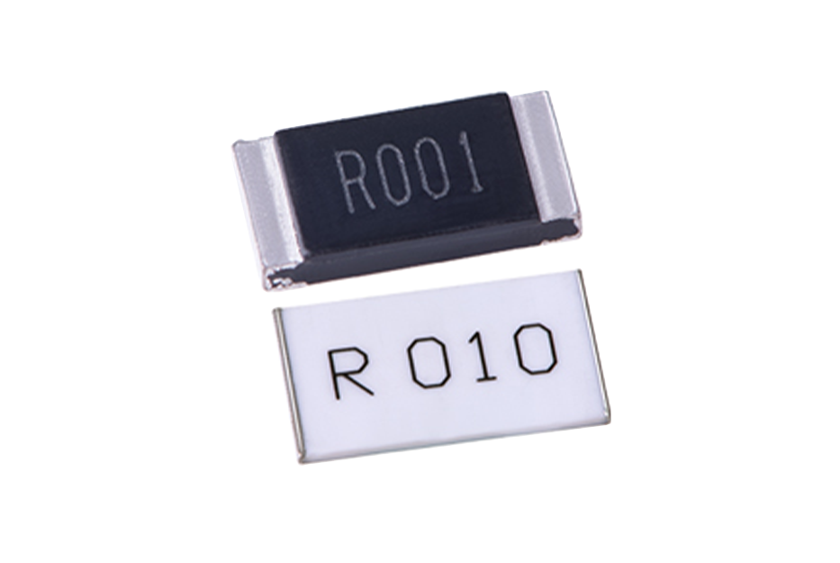
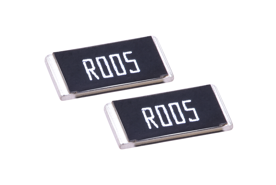

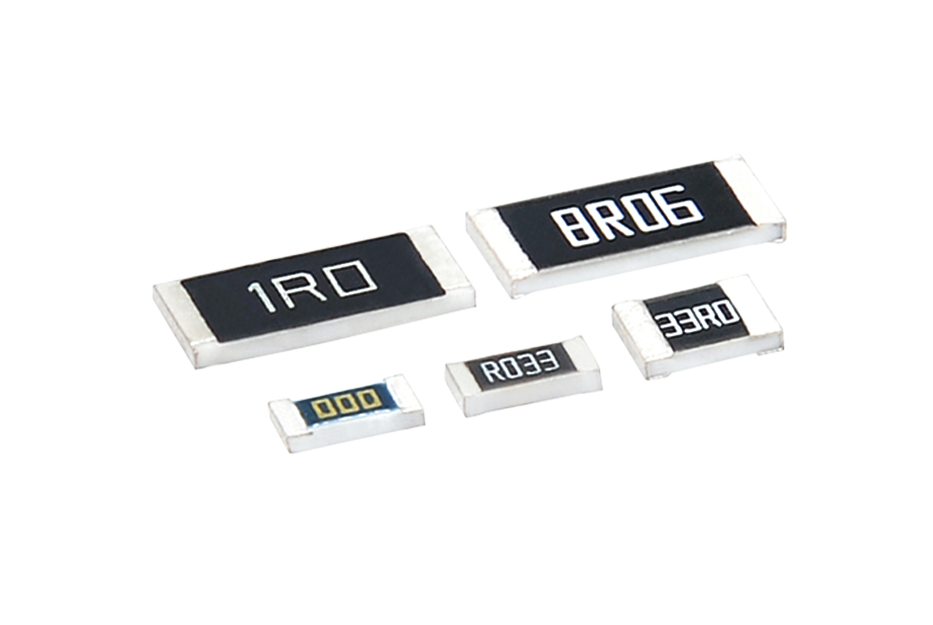


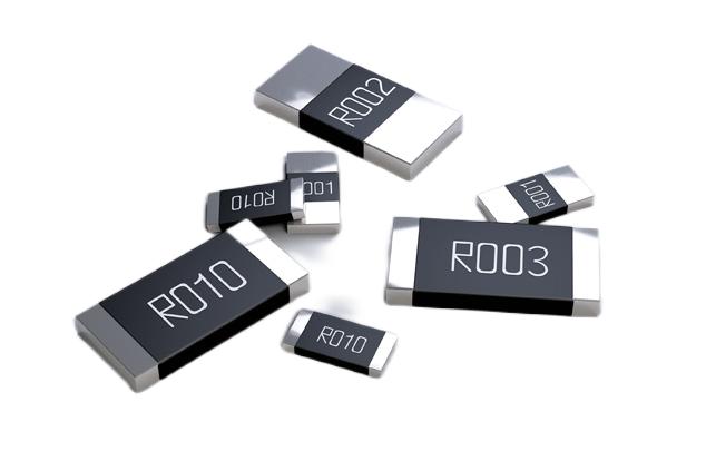


Rom wafer resistors are one of the commonly used components in integrated circuits, and their conductivity directly affects the efficiency of the entire circuit. In the design and manufacturing process, optimizing the conductivity of Rom wafer resistors is very important. At present, commonly used Roma wafer resistance materials include metal copper, alloy nickel chromium, resistance paint, and carbon film. Reasonable selection of suitable materials is essential for different application scenarios. For example, in high-frequency applications, alloy nickel chromium resistance materials have good conductivity and high-temperature resistance, which can better meet the needs of high-frequency circuits.

Developing materials with high conductivity is also an important direction for optimizing the conductivity of Roma wafer resistors. For example, graphene materials have extremely high conductivity and can serve as a conductive layer for Rom wafer resistors. By adding graphene to the Rom wafer resistor material, the conductivity of the Rom wafer resistor can be improved, thereby increasing the efficiency of the circuit. The conductive layer of the Rom wafer resistor is usually covered on the substrate in a certain pattern form. By reasonably designing the shape, size, and layout of conductive patterns, the resistance of the conductive layer can be reduced and the conductivity can be improved. For example, using a folded conductive layer can increase the length of the conductive path, thereby reducing the resistance value and improving conductive efficiency. When preparing Roma wafer resistors, the deposition, photolithography, and corrosion processes of the resistive material can have an impact on the conductivity. Therefore, optimizing the preparation process reasonably to ensure the uniformity and integrity of the conductive layer can improve the conductivity of the Roma wafer resistor.

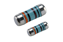
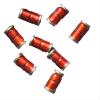
CSR0207JTDU03R9
MELF Metal Film Resistor ,0207 ,3.9R ,±5% ,1/2W ,±50PPM ,ELLON-CSR

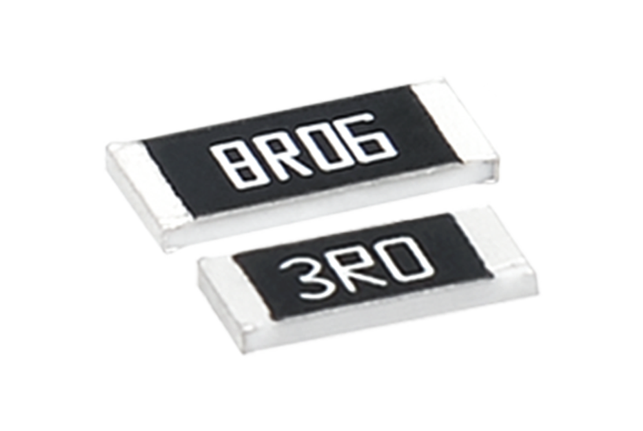
CSR0204DTDV2200
MELF Metal Film Resistor ,0204 ,220R ,±0.5% ,1/4W(0.25W) ,±50PPM ,ELLON-CSR
Reasonable size design can also improve the influence of the thickness and area of the conductive layer on resistance. Generally, the thinner the thickness of the conductive layer, the smaller the resistance value; The larger the area of the conductive layer, the smaller the resistance value. Therefore, when designing Rom wafer resistors, it is necessary to reasonably select the thickness and area of the conductive layer based on specific application needs to improve conductivity.
Optimizing the conductivity of Roma wafer resistors can improve circuit efficiency, and can also improve the conductivity of Roma wafer resistors by selecting appropriate materials, developing new materials, optimizing the conductive layer structure, improving preparation processes, and designing reasonable sizes, thereby improving circuit efficiency. With the continuous progress and development of technology, we believe that we can continuously seek better methods and technologies to further optimize the conductivity of Roma wafer resistors and achieve continuous improvement in circuit efficiency.